- About ripple carry adder
- About
- Ripple carry adder
- Ripple carry adder circuit.
- Full adder.
- Full adder using NAND or NOR logic.
- Ripple-Carry Adder
- Related terms:
- Processing Elements
- Ripple-Carry Adder
- Number Representation and Computer Arithmetic
- VII Fast Adders
- Two-Operand Addition
- 2.11 Two’s Complement and Ones’ Complement Adders
- Fault Tolerance in Computer Systems—From Circuits to Algorithms*
- Adder and Multiplier Applications
- Computer arithmetic
- 4.4 Fast adders*
- Logic synthesis in a nutshell
- 6.5.2 Functional timing analysis
- 6.5.2.1 Delay models and modes of operation
- 6.5.2.2 True floating mode delay
- Introducing parallel and distributed computing concepts in digital logic
- 5.4.1 Adders
- Combinational logic circuits
- Ripple carry adder
- Digital Building Blocks
- Prefix Adder*
About ripple carry adder
An example of how an abstract operation (addition) can be performed by a physical system.
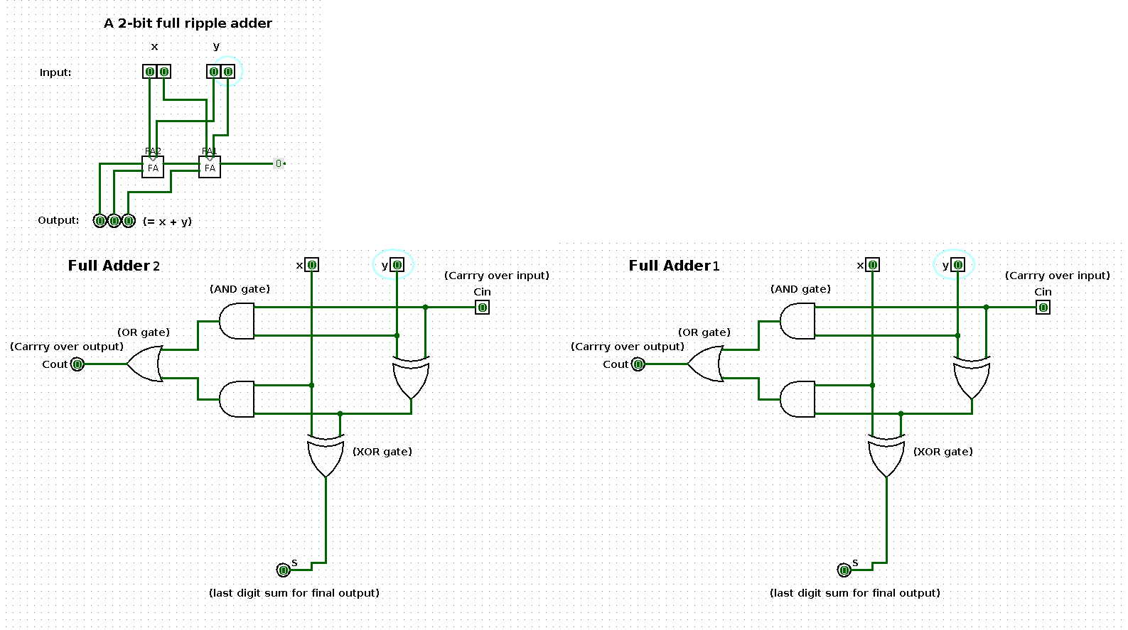
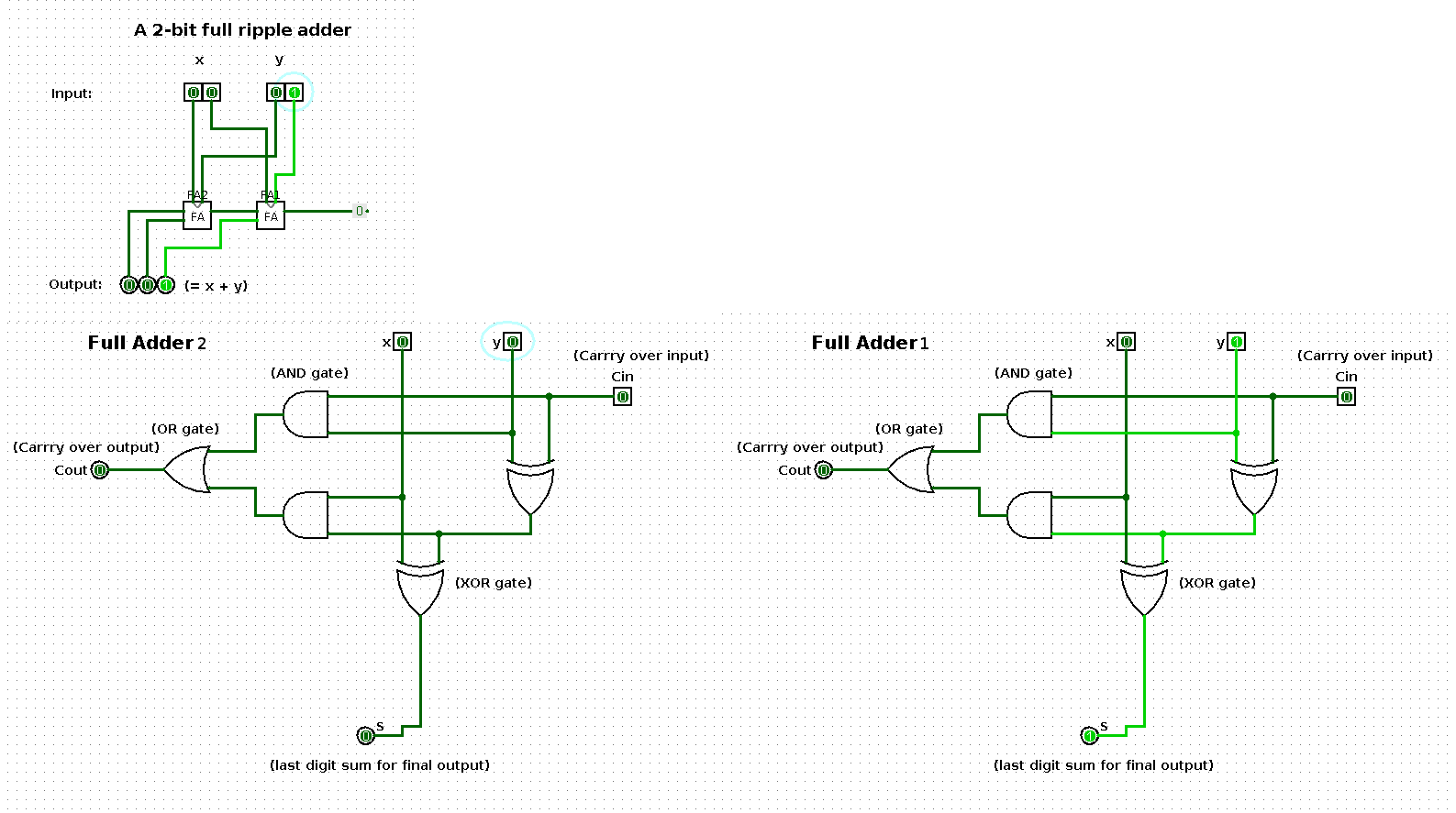
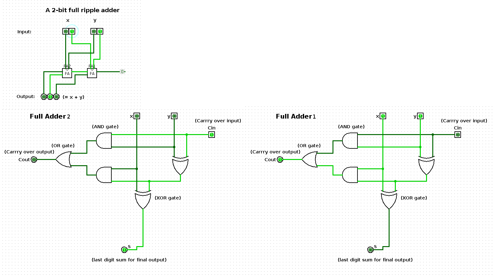
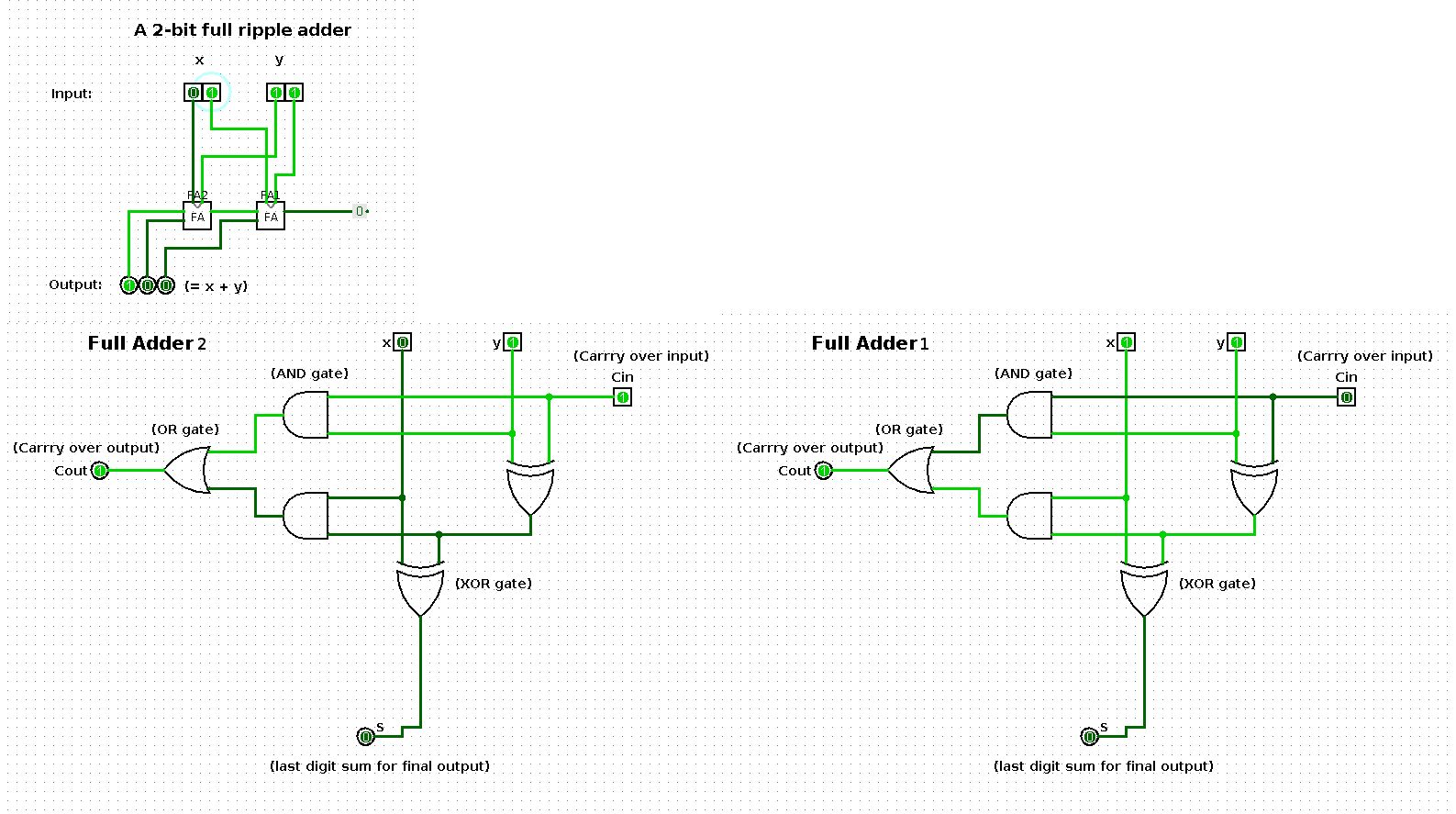
The following shows a sequence of additions performed by a 2-bit input based ripple-carry adder (full ripple adder). Per step in the sequence one of the operands is increased by one such that the result shows a binary count from 0 up and until 100.

The two large images at the bottom represent the respective boxes in the middle of the ripple-carry adder in the top left image.
Click on the image to see it enlarged. Also see the following:
You can play with the logical circuit yourself by opening the two_bit_input_ripple_carry_adder.circ file in logisim.
What is this thing?
This ‘thing’ in the image above shows an abstract circuit for a ripple-carry adder.
A ripple-carry adder is a particular type of implementation of the component of a computer that enables it to perform addition.
The 0 and 1 signals per binary digit from x and y are physically implemented by the respective absence and presence of an electric current.
The AND, OR and XOR gates are called logical gates. These are abstractions that can be implemented in the real world using electronic components. It is useful to use abstractions because we want to be able to decouple these concepts from a specific implementation. For one because there are multiple ways these logical gates can be physically implemented.
To find out more about these logical gates and how they can be physically implemented, see here.
To get an idea how the ripple-carry adder fits into the design of a computer, see here.
States in the sequence
State 0
| x | y | x + y |
|---|---|---|
| 0 | 0 | 0 |
State 1
| x | y | x + y |
|---|---|---|
| 0 | 1 | 1 |
State 2
| x | y | x + y |
|---|---|---|
| 1 | 1 | 10 |
State 3
| x | y | x + y |
|---|---|---|
| 1 | 10 | 11 |

State 4
| x | y | x + y |
|---|---|---|
| 1 | 11 | 100 |
Tools used to create the sequence
- logisim (to implement logical circuits)
- shutter (to take screenshots)
- gimp (to compose shots in one image)
- convert (for gif creation)
- kazam (for video creation)
About
An example of how an abstract operation (addition) can be performed by a physical system.
Источник
Ripple carry adder
In this article, learn about Ripple carry adder by learning the circuit. A ripple carry adder is an important digital electronics concept, essential in designing digital circuits.
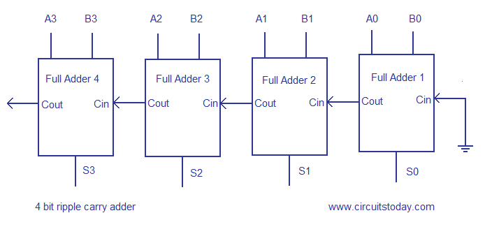
Ripple carry adder circuit.
Multiple full adder circuits can be cascaded in parallel to add an N-bit number. For an N- bit parallel adder, there must be N number of full adder circuits. A ripple carry adder is a logic circuit in which the carry-out of each full adder is the carry in of the succeeding next most significant full adder. It is called a ripple carry adder because each carry bit gets rippled into the next stage. In a ripple carry adder the sum and carry out bits of any half adder stage is not valid until the carry in of that stage occurs.Propagation delays inside the logic circuitry is the reason behind this. Propagation delay is time elapsed between the application of an input and occurance of the corresponding output. Consider a NOT gate, When the input is “0” the output will be “1” and vice versa. The time taken for the NOT gate’s output to become “0” after the application of logic “1” to the NOT gate’s input is the propagation delay here. Similarly the carry propagation delay is the time elapsed between the application of the carry in signal and the occurance of the carry out (Cout) signal. Circuit diagram of a 4-bit ripple carry adder is shown below.
 Ripple carry adder
Sum out S0 and carry out Cout of the Full Adder 1 is valid only after the propagation delay of Full Adder 1. In the same way, Sum out S3 of the Full Adder 4 is valid only after the joint propagation delays of Full Adder 1 to Full Adder 4. In simple words, the final result of the ripple carry adder is valid only after the joint propogation delays of all full adder circuits inside it.
Full adder.
To understand the working of a ripple carry adder completely, you need to have a look at the full adder too. Full adder is a logic circuit that adds two input operand bits plus a Carry in bit and outputs a Carry out bit and a sum bit.. The Sum out (Sout) of a full adder is the XOR of input operand bits A, B and the Carry in (Cin) bit. Truth table and schematic of a 1 bit Full adder is shown below
There is a simple trick to find results of a full adder. Consider the second last row of the truth table, here the operands are 1, 1, 0 ie (A, B, Cin). Add them together ie 1+1+0 = 10 . In binary system, the number order is 0, 1, 10, 11……. and so the result of 1+1+0 is 10 just like we get 1+1+0 =2 in decimal system. 2 in the decimal system corresponds to 10 in the binary system. Swapping the result “10” will give S=0 and Cout = 1 and the second last row is justified. This can be applied to any row in the table.
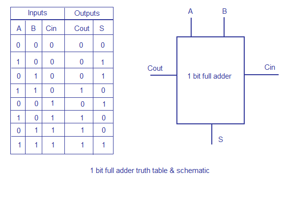 1 bit full adder schematic and truth table
A Full adder can be made by combining two half adder circuits together (a half adder is a circuit that adds two input bits and outputs a sum bit and a carry bit).
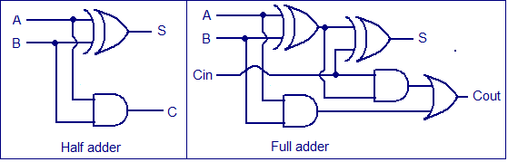 Full adder & half adder circuit
Full adder using NAND or NOR logic.
Alternatively the full adder can be made using NAND or NOR logic. These schemes are universally accepted and their circuit diagrams are shown below.
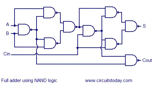 Full adder using NAND logic
 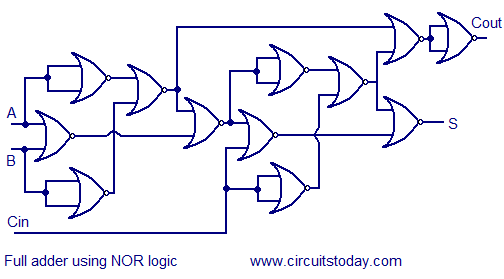 Full adder using NOR logic
Источник
Ripple-Carry Adder
Related terms:
Download as PDF
About this page
Processing Elements
Lars Wanhammar , in DSP Integrated Circuits , 1999
Ripple-Carry Adder
The ripple-carry adder (RCA) is the simplest form of adder [ 22 ]. Two numbers using two’s-complement representation can be added by using the circut shown in Figure 11.3 . A Wd-bit RCA is built by connecting Wd full-adders so that the carry-out from each full-adder is the carry-in to the next stage. The sum and carry bits are generated sequentially, starting from the LSB. The carry-in bit into the rightmost full-adder, corresponding to the LSB, is set to zero, i. e., (cWd = 0). The speed of the RCA is determined by the carry propagation time which is of order O(Wd). Special circuit realization of the full-adders with fast carry generation are often employed to speed the operation. Pipelining can also be used.

Figure 11.3 . Ripple-carry adder
Figure 11.4 shows how a 4-bit RCA can be used to obtain an adder/sub-tractor. Subtraction is performed by adding the negative value. The subtrahend is bit-complemented and added to the minuend while the carry into the LSB is set to 1 (cWd = 1).

Figure 11.4 . Ripple-carry adder/subtractor
Addition time is essentially determined by the carry path in the full-adders. Notice that even though the adder is said to be bit-parallel, computation of the output bits is done sequentially. In fact, at each time instant only one of the full-adders performs useful work. The others have already completed their computations or may not yet have received a correct carry input, hence they may perform erroneous computations. Because of these wasted switch operations, power consumption is higher than necessary.
Number Representation and Computer Arithmetic
VII Fast Adders
Ripple-carry adders are quite simple and easily expandable to any desired width. However, they are rather slow, because carries may propagate across the full width of the adder. This happens, for example, when the two 8-bit numbers 10101011 and 01010101 are added. Because each FA requires some time to generate its carry output, cascading k such units together implies k times as much signal delay in the worst case. This linear amount of time becomes unacceptable for wide words (say, 32 or 64 bits) or in high-performance computers, though it might be acceptable in an embedded system that is dedicated to a single task and is not expected to be fast.
A variety of fast adders can be designed that require logarithmic, rather than linear, time. In other words, the delay of such fast adders grows as the logarithm of k. The best-known and most widely used such adders are carry-lookahead adders. The basic idea in carry-lookahead addition is to form the required intermediate carries directly from the inputs rather than from the previous carries, as was done in Fig. 6 . For example, the carry c3 in Fig. 6 , which is normally expressed in terms of c2 using the carry recurrence
can be directly derived from the inputs based on the logical expression:
To simplify the rest of our discussion of fast adders, we define the carry generate and carry propagate signals and use them in writing a carry recurrence that relates ci+1 to ci:
The expanded form of c3, derived earlier, now becomes:
It is easy to see that the expanded expression above would grow quite large for a wider adder that requires c31 or c52, say, to be derived. A variety of lookahead carry networks exist that systematize the preceding derivation for all the intermediate carries in parallel and make the computation efficient by sharing parts of the required circuits whenever possible. Various designs offer trade-offs in speed, cost, layout area (amount of space on a VSLI chip needed to accomodate the required circuit elements and wires that interconnect them), and power consumption. Information on the design of fast carry networks and other types of fast adders can be found in books on computer arithmetic.
Here, we present just one example of a fast carry network. The building blocks of this network are the carry operator which combines the generate and propagate signals for two adjacent blocks [i + 1, j] and [h, i] of digit positions into the respective signals for the wider combined block [h, j]. In other words
where [a, b] stands for (g[a,b], P[a,b]) representing the pair of generate and propagate signals for the block extending from digit position a to digit position b. Because the problem of determining all the carries ci is the same as computing the cumulative generate signals g[o,i], a network built of ¢ operator blocks, such as the one depicted in Fig. 8 , can be used to derive all the carries in parallel. If a cin signal is required for the adder, it can be accommodated as the generate signal g−1 of an extra position on the right.

Figure 8 . Brent-Kung lookahead carry network for an 8-digit adder.
For a k-digit adder, the number of operator blocks on the critical path of the carry network exemplified by Fig. 8 is 2(⌈log2 k⌉−1). Many other carry networks can be designed that offer speed-cost trade-offs.
An important method for fast adder design, that often complements the carry-lookahead scheme, is carry-select. In the simplest application of the carry-select method, a k-bit adder is built of a (k/2)-bit adder in the lower half, two (k/2)-bit adders in the upper half (forming two versions of the k/ 2 upper sum bits with ck/2 = 0 and ck/2 = 1), and a multiplexer for choosing the correct set of values once ck/2 becomes known. A hybrid design, in which some of the carries (say, c8, c16, and c24 in a 32-bit adder) are derived via carry-lookahead and are then used to select one of two versions of the sum bits that are produced for 8-bit blocks concurrently with the operation of the carry network, is quite popular in modern arithmetic units.
Two-Operand Addition
Miloš D. Ercegovac , Tomás Lang , in Digital Arithmetic , 2004
2.11 Two’s Complement and Ones’ Complement Adders
We have discussed several adder schemes for addition of positive integers (actually unsigned fixed-point numbers) in a radix-2 representation. We now discuss how these adders are used for addition of signed numbers in two’s complement and ones’ complement representations.
As shown in Chapter 1 , the use for two’s complement representation is straightforward: the n-bit sum output of the adder is the result, and the carry-out is discarded. Moreover, the overflow is detected from the most-significant bits of the operands and the result.
For ones’ complement addition it is necessary to add the carry-out. We now consider how this addition is done for a carry-ripple adder and for a prefix adder.
For a carry-ripple adder the carry-out is connected to the carry-in (end-around carry) as shown in Figure 1.3 . This produces a combinational network with a loop, so that a sequential behavior or oscillations can occur. To study this issue we consider two situations:
The operands have at least one position in which xi, ⊕ yi = 0. In such a case, the carry loop is initiated and terminates in that position, effectively breaking the loop. In the following example this occurs for position 3.
All positions are such that xi ⊕ yi = 1. In this case, the result of the addition corresponds to the value 0. The actual representation of the sum depends on the value of the carry in the loop: if it is 0, then the output is 111 … 1, and if it is 1, the output is 000 … 0, which both represent 0 in ones’ complement.
However, in this case there might be an oscillation. This occurs if initially (when the operation is initiated) some carries are 1 and others are 0. This pattern of carries goes around the loop producing an oscillation in the output. To avoid this oscillation it is necessary to set the initial carries to a common value (either all 0 or all 1). This requires a “preset” phase in the operation of the adder.
The fact that the carry chain is effectively broken by a pair for which xi ⊕ yi =0 indicates that the delay of this modified adder is the same as the delay of the carry-ripple adder, since the worst-case delay is still determined by a carry propagation through n − 1 full-adders.
For the prefix adder, the end-around carry approach could also be used. However, if the carry-in is included at the top of the array, as shown for instance in Figure 2.20 , this end-around carry would significantly increase the delay (see Exercise 2.31 ). Consequently, a modification of the adder is more effective, in which the carry-in is added in an additional level. Figure 2.29 shows the resulting adder. Note the high load on the end-around carry signal, which affects the overall delay.

FIGURE 2.29 . Implementing ones’ complement adder with prefix network. (Modules to obtain pi, gi, and ai, signals not shown.)
Fault Tolerance in Computer Systems—From Circuits to Algorithms*
Shantanu Dutt , . Fran Hanchek , in The Electrical Engineering Handbook , 2005
Adder and Multiplier Applications
The REMOD method was applied to a ripple-carry adder , which consist of fully dependent linearly connected cells (Dutt and Hanchek, 1997). The cells are either 1-bit or 4-bit carry look-ahead (CLA) adders. REMOD was also applied to multipliers based on a Wallace tree and on a carry-save array for the summation of partial product terms (Dutt and Hanchek, 1997). The multipliers are partitioned into arrays of independent subcells, but the high time overhead normally associated with independent cells is masked through a clever application of REMOD. Original and checking computations overlap in time between adjacent rows of subcells as the computations proceed down the array or Wallace tree. The designs were laid out using the Berkeley MAGIC tools for CMOS. The multiplier designs were implemented in CMOS dynamic logic. Delay elements were implemented as strings of inverters. Error injection gates were inserted into the layout to simulate stuck-at faults. The layout tools allow geometry information to be extracted and converted to SPICE parameters. Simulations of the circuits using delay element pipelining were then performed using HSPICE. The simulations successfully tested the functions of error detection and reconfiguration, with selected nodes in the SPICE files for the circuits forced to logic high or low to simulate faults.
Computer arithmetic
4.4 Fast adders*
A great deal of effort has gone into the design of ALU circuits that operate faster than those based on the ripple carry adder. We have noted earlier that the ripple carry adder is slow because each adder stage can form its outputs only when all the earlier stages have produced theirs 2 . Since stage i produces a carry-out bit, Ci+1, that depends on the inputs Ai, Ti, and Ci, it is possible to obtain logic equations for the carry-out from each stage.
Our first attempt is to use the relationship derived earlier:
Putting i = 0, we have:
Putting i = 1, we have:
Similarly, we can write expressions for C3, C4, and so on. Theoretically, these expressions allow us to design a logic circuit to produce all the carry signals at the same time using two layers of gates. Unfortunately, the expressions become extremely long; give a thought to how the expression for C31 would look! We do not pursue this possible solution any further because the number of gates becomes extremely large.
Our second attempt at a solution will result in a practical fast adder. The so-called carry-look-ahead 3 ALU generates all the carry signals at the same time, although not as quickly as our first attempt would have done. Reconsider the truth table for the adder, Figure 4.3 . Note that when Ai and Ti have different values, the carry-out from the adder stage is the same as the carry-in. That is, when Ai./Ti + /Ai.TI = = 1, then Ci+1 = Ci; we regard this as the carry-in ‘propagating’ to the carry-out. Also, when Ai and Ti are both 1, Ci+1 = 1, that is, when Ai.Ti = = 1, then Ci+1 = 1; we regard this as the carry-out being ‘generated’ by the adder stage. Putting these expressions together, we have:
This can be simplified to:
This is really a formal statement of common sense. The carry-out, Ci+1, is 1 if the carry-in, Ci , is a 1 AND the stage propagates the carry through the stage OR if the carry-out is set to 1 by the adder stage itself. At first sight, this does not appear to be an improvement over the ripple-carry adder . However, we persevere with the analysis; putting i = 0, 1, 2, 3, …, we obtain:
We can readily make a 4-bit adder from these equations. However, the equations are becoming rather large, implying that a large number of gates will be required to produce C31. To overcome this difficulty, let us regard a 4-bit adder as a building block, and use four of them to make a 16-bit adder. We could simply connect the carry-out of each 4-bit adder to the carry-in of the next 4-bit adder, as shown in Figure 4.11(a) . In this case, we are using a ripple-carry between the 4-bit blocks. Alternatively, we can regard each 4-bit block as either generating or propagating a carry, just as we did for the 1-bit adders. This allows us to devise carry-look-ahead logic for the carry-in signals to each 4-bit adder block, as shown in Figure 4.11(b) . (The logic equations turn out to be the same as that for the 1-bit adders.) We now have a 16-bit adder made from four blocks of 4-bit adders with carry-look-ahead logic. Wider adders can be made by regarding the 16-bit adder as a building block and, again, similar logic allows us to produce carry-look-ahead circuits for groups of 16-bit adders. Even though there are now several layers of look-ahead logic, this adder has a substantial advantage in speed of operation when compared with the ripple-carry-adder. As is often the case, this speed advantage is at the expense of a more complex circuit.

Figure 4.11 . (a) Ripple-carry between groups; (b) carry look-ahead over the groups
Logic synthesis in a nutshell
Jie-Hong (Roland) Jiang , Srinivas Devadas , in Electronic Design Automation , 2009
6.5.2 Functional timing analysis
The problem with topological analysis of a circuit is that not all critical paths in a circuit need be responsible for the circuit delay. Critical paths in a circuit can be false, i.e., not responsible for the delay of a circuit. The critical delay of a circuit is defined as the delay of the longest true path in the circuit. Thus, if the topologically longest path in a circuit is false, then the critical delay of the circuit will be less than the delay of the longest path. The critical delay of a combinational logic circuit is dependent on not only the topological interconnection of gates and wires, but also the Boolean functionality of each node in the circuit. Topological analysis only gives a conservative upper bound on the circuit delay.
Assume the fixed delay model, and consider the carry bypass circuit of Figure 6.33 . The circuit uses a conventional ripple-carry adder (the output of gate 11 is the ripple-carry output) with an extra AND gate (gate 10) and an additional multiplexor. If the propagate signals p0 and p1 (the outputs of gates 1 and 3, respectively) are high, then the carry-out of the block c2 is equal to the carry-in of the block c0. Otherwise it is equal to the output of the ripple-carry adder. The multiplexor thus allows the carry to skip the ripple-carry chain when all the propagate bits are high. A carry-bypass adder of arbitrary size can be constructed by cascading a set of individual carry-bypass adder blocks, such as those of Figure 6.33 .

FIGURE 6.33 . 2-bit carry-bypass adder.
Assume the primary input c0 arrives at time t = 5 and all the other primary inputs arrive at time t = 0. Let us assign a gate delay of 1 for AND and OR gates and gate delays of 2 for the XOR gates and the multiplexor. The longest path including the late arriving input in the circuit is the path shown in bold, call it P, from c0 to c2 through gates 6, 7, 9, 11, and the multiplexor (the delay of this path is 11). A transition can never propagate down this path to the output because in order for that to happen the propagate signals have to be high, in which case the transition propagates along the bypass path from c0 through the multiplexor to the output. This path is false since it cannot be responsible for the delay of the circuit.
For this circuit, the path that determines the worst-case delay of c2 is the path from a0 to c2 through gates 1, 6, 7, 9, 11, and the multiplexor. The output of this critical path is available after 8 gate delays. The critical delay of the circuit is 8 and is less than the longest path delay of 11.
6.5.2.1 Delay models and modes of operation
Whether a path is a true or false delay path closely depends on the delay model and the mode of operation of a circuit.
In the commonly used fixed delay model, the delay of a gate is assumed to be a fixed number d, which is typically an upper bound on the delay of the component in the fabricated circuit. In contrast, the monotone speedup delay model takes into account the fact that the delay of each gate can vary. It specifies the delays as an interval [O, d], with the lower bound O and upper bound d on the actual delay.
Consider the operation of a circuit over the period of application of two consecutive input vectors v1 and v2. In the transition mode of operation, the circuit nodes are assumed to be ideal capacitors and retain their values set by v1 until v2 forces the voltage to change. Thus, the timing response for v2 is also a function of v1 (and possibly other previously applied vectors). In contrast, in the floating mode of operation the nodes are not assumed to be ideal capacitors, and hence their state is unknown until it is set by v2. Thus, the timing behavior for v2 is independent of v1.
Transition Mode and Monotone Speedup. In our analysis of the carry-bypass adder we assumed fixed delays for the different gates in the circuit and applied a vector pair to the primary inputs. It was clear that an event (a signal transition, either 0 → 1 or 1 → 0) could not propagate down the longest path in the circuit. A precise characterization is that the path cannot be sensitized, and thus false, under the transition mode of operation and under (the given) fixed gate delays. Varying the gate delays in Figure 6.33 does not change the sensitizability of the path shown in bold.
False path analysis under the fixed delay model and the transition mode of operation, however, may be problematic as seen from the following example.
Consider the circuit of Figure 6.34a , taken from [ McGeer 1989 ]. The delays of each of the gates are given inside the gates. In order to determine the critical delay of the circuit we will have to simulate the two vector pairs corresponding to a, making a 0 → 1 transition and a 1 → 0 transition. Applying 0 → 1 and 1→ 0 transitions on a does not change the output f from 0. Thus, one can conclude that the circuit has critical delay 0 under the transition mode of operation for the given fixed gate delays.

FIGURE 6.34 . Transition mode with fixed delays.
Now consider the circuit of Figure 6.34b which is identical to the circuit of Figure 6.34a except that the buffer at the input to the NOR gate has been sped up from 2 to 0. We might expect that speeding up a gate in a circuit would not increase the critical delay of a circuit. However, for the 0 → 1 transition on a, the output f switches both at time 5 and time 6, and the critical delay of the circuit is 6.
This example shows that a sensitization condition based on transition mode and fixed gate delays is unacceptable in the worst-case design methodology, where we are given the upper bounds on the gate delays and are required to report the (worst-case) critical path in the circuit. Unfortunately, if we use only the upper bounds of gate delays under the transition mode of operation, an erroneous critical delay may be computed.
To obtain a useful sensitization condition, one strategy is to use the transition mode of operation and monotone speedup as the following example illustrates.
Consider the circuit of Figure 6.35 , which is identical to the circuit of Figure 6.34a , except that each gate delay can vary from 0 to its given upper bound. As before, in order to determine the critical delay of the circuit, we will have to simulate the two vector pairs corresponding to a making a 0 → 1 transition and a 1 → 0 transition. However, the process of simulating the circuit is much more complicated since the transitions at the internal gates may occur at varying times. In the figure, the possible combinations of waveforms that appear at the outputs of each gate are given for the 0 → 1 transition on a. Fa instance, the NOR gate can either stay at 0 or make a 0 → 1 → 0 transition, where the transitions can occur between [0,3] and [0,4], respectively. In order to determine the critical delay of the circuit, we scan all the possible waveforms at output f and find the time at which the last transition occurs over all the waveforms. This analysis provides us with a critical delay of 6.

FIGURE 6.35 . Transition mode with monotone speedup.
Timing analysis for a worst-case design methodology can use the above strategy of monotone speedup delay simulation under the transition mode of operation. The strategy however has several disadvantages. Firstly, the search space is 2 2n where n is the number of primary inputs to the circuit, since we may have to simulate each possible vector pair. Secondly, monotone speedup delay simulation is significantly more complicated than fixed delay simulation. These difficulties have motivated delay computation under the floating mode of operation.
Floating Mode and Monotone Speedup. Under floating mode, the delay is determined by a single vector. As compared to transition mode, critical delay under floating mode is significantly easier to compute for the fixed or monotone speedup delay model because large sets of possible waveforms do not need to be stored at each gate. Single-vector analysis and floating mode operation, by definition, make pessimistic assumptions regarding the previous state of nodes in the circuit. The assumptions made in floating mode operation make the fixed delay model and the monotone speedup delay model equivalent. 3
6.5.2.2 True floating mode delay
The necessary and sufficient condition for a path to be responsible for circuit delay under the floating mode of operation is a delay-dependent condition.
The fundamental assumptions made in single-vector delay-dependent analysis are illustrated in Figure 6.36 . Consider the AND gate of Figure 6.36a . Assume that the AND gate has delay d and is embedded in a larger circuit, and a vector pair (v1, v2) is applied to the circuit inputs, resulting in a rising transition occurring at time t1 on the first input to the AND gate and a rising transition at time t2 on the second input. The output of the gate rises at a time given by max<t1, t2> + d. The abstraction under floating mode of operation only shows the value of v2. In this case a 1 arrives at the first and second inputs to the AND gate at times t1 and t2, respectively, and a 1 appears at the output at time max <t1, t2> + d. Similarly, in Figure 6.36b two falling transitions at the AND gate inputs result in a falling transition at the output at a time that is the minimum of the input arrival times plus the delay of the gate.

FIGURE 6.36 . Fundamental assumptions made in floating mode operation.
Now consider Figure 6.36c , where a rising transition occurs at time t1 on the first input to the AND gate and a falling transition occurs at time t2 on the second input. Depending on the relationship between t1 and t2 the output will either stay at 0 (for t1 ≥ t2) or glitch to a 1 (for t1 Figure 6.35 .) However, under the floating mode of operation we only have the vector v2. The 1 at the first input to the AND gate arrives at time t1, and the 0 at the second input arrives at time t2. The output of the AND on v2 obviously settles to 0 on v2, but at what time does it settle? If t1 ≥ t2, then the output of the gate is always 0, and the 0 effectively arrives at time 0. If t1 Figure 6.36 represent a timed calculus for single-vector simulation with delay values that can be used to determine the correct floating mode delay of a circuit under an applied vector v2 (assuming pessimistic unknown values for v1) and the paths that are responsible for the delay under v2. The rules can be generalized as follows:
If the gate output is at a controlling value, pick the minimum among the delays of the controlling values at the gate inputs. (There has to be at least one input with a controlling value. The non-controlling values are ignored.) Add the gate delay to the chosen value to obtain the delay at the gate output.
If the gate output is at a non-controlling value, pick the maximum of all the delays at the gate inputs. (All the gate inputs have to be at non-controlling values.) Add the gate delay to the chosen value to obtain the delay at the gate output.
To determine whether a path is responsible for floating mode delay under a vector v2, we simulate v2 on the circuit using the timed calculus. As shown in [ Chen 1991 ], a path is responsible for the floating mode delay of a circuit on v2 if and only if for each gate along the path:
If the gate output is at a controlling value, then the input to the gate corresponding to the path has to be at a controlling value and furthermore has to have a delay no greater than the delays of the other inputs with controlling values.
If the gate output is at a non-controlling value, then the input to the gate corresponding to the path has to have a delay no smaller than the delays at the other inputs.
Let us apply the above conditions to determine the delay of the following circuits.
Consider the circuit of Figure 6.34a reproduced in Figure 6.37 . Applying the vector a = 1 sensitizes the path of length 6 shown in bold, illustrating that the sensitization condition takes into account monotone speedup (unlike transition mode fixed delay simulation). Each wire has both a logical value and a delay value (in parentheses) under the applied vector.

FIGURE 6.37 . First example of floating mode delay computation on a circuit.
Consider the circuit of Figure 6.38 . Applying the vector (a, b, c) = (0, 0, 0) gives a floating mode delay of 3. The paths

FIGURE 6.38 . Second example of floating mode delay computation on a circuit.
Consider the circuit of Figure 6.39 . Applying a = 0 and a = 1 results in a floating mode delay of 5.

FIGURE 6.39 . Third example of floating mode delay computation on a circuit.
We presented informal arguments justifying the single-vector abstractions of Figure 6.36 to show that the derived sensitization condition is necessary and sufficient for a path to be responsible for the delay of the circuit under the floating mode of operation. For a topologically oriented formal proof of the necessity and sufficiency of the derived condition, see [ Chen 1991 ].
Introducing parallel and distributed computing concepts in digital logic
Ramachandran Vaidyanathan , . Suresh Rai , in Topics in Parallel and Distributed Computing , 2015
5.4.1 Adders
Adders are one of the most commonly discussed combinational circuits in a course on digital logic and offer unique opportunities for exploring PDC topics. Consider the standard ripple-carry adder illustrated in Figure 5.12 . The bottleneck of the ripple-carry adder’s speed is the sequential generation of carry bits—that is, the longest path in the circuit traverses the carry lines. Students should note the important design principle of improving overall performance of a module by reducing its bottleneck (or critical path). This principle can also be seen as being somewhat similar to Amdahl’s law [ 26 , 27 ], which states that the part of an algorithm that is inherently sequential is the speed bottleneck in parallelizing this algorithm. For the ripple-carry adder (all of whose component full adders run in parallel) the carry generation used reflects an inherently sequential task. Here the speed of the circuit is bottlenecked by this sequential part (namely, ripple-carry generation).

Figure 5.12 . A four-bit ripple-carry adder. Each box labeled “FA” is a full adder accepting data bits ai and bi and carry-in bit ci, and generating the sum bit si and the carry-out bit ci+1.
In the normal course of explaining a ripple-carry adder, one would note that for i ≥ 0, the (i + 1)th carry ci+1 is given by the following recurrence in which “+” and “⋅” represent the logical OR and AND operations.
Here ai and bi are the ith bits of the numbers to be added, and gi and pi are the ithcarry-generate and carry-propagate bits. Given this first-order recurrence in which ci+1 is expressed using ci, a student in a first digital logic class (typically a freshman or sophomore) may incorrectly assume that carry computation (or for that matter any recurrence) is inherently sequential and that the adder circuit cannot overcome the delay of a ripple-carry adder. This presents the opportunity to use a carry-look-ahead adder ( Figure 5.13 ) to show how seemingly sequential operations can be parallelized. In particular, one could introduce the idea of parallel prefix, a versatile PDC operation used in numerous applications ranging from polynomial evaluation and random number generation to the N-body problem and genome sequence alignment [ 28 , 29 ].

Figure 5.13 . A four-bit carry-look-ahead adder. Each box labeled “FA” is a modified full adder accepting data bits ai and bi and carry-in bit ci, and generating the sum bit si and the carry-generate and carry-propagate bits gi and pi.
A prefix computation is a special case of a first-order recurrence in that βi = βi−1 ⊗ αi. We now develop the relationship in the other direction and indicate how the first-order recurrence for the carry in Equation ( 5.1 ) can be expressed as a prefix computation.
Let x1, y1, x2, and y2 be four binary signals. Define a binary operation ⊙ on two doublets (pairs) x 1 , y 1 and x 2 , y 2 to produce the doublet x , y = x 1 , y 1 ⊙ x 2 , y 2 defined as follows:
where + and ⋅ denote the OR and AND operations. The operation ⊙ can be proved to be associative. It can be shown that for j ≥ 0 and doublets x j , y j ,
Notice that this represents a prefix computation on the doublets x i , y i with respect to the operation ⊙.
The ripple-carry circuit corresponds to a very slow prefix computation. A carry-look-ahead adder employs a fast prefix computation circuit to generate the carry bits. In general, by adopting different prefix circuits for carry generation, one could create adders with different cost-performance trade-offs. In Section 5.5.1 we will revisit prefix computations in the context of counters. It should also be noted that, in general, any linear recurrence can be converted to a prefix computation [ 30 , 31 ].
Combinational logic circuits
John Crowe , Barrie Hayes-Gill , in Introduction to Digital Electronics , 1998
Ripple carry adder
The ripple carry, or parallel adder, arises out of considering how we perform addition, and is therefore a heuristic solution. Two numbers can be added by beginning with the two least significant digits to produce their sum, plus a carry-out bit (if necessary). Then the next two digits are added (together with any carry-in bit from the addition of the first two digits) to produce the next sum digit and any carry-out bit produced at this stage. This process is then repeated until the most significant digits are reached (see Section 2.5.1 ).
To implement this procedure, for binary arithmetic, what is required is a logic block which can take two input bits, and add them together with a carry-in bit to produce their sum and a carry-out bit. This is exactly what the full adder, described earlier in Section 4.1.5 , does. Consequently by joining four full adders together, with the carry-out from one adder connected to the carry-in of the next, a four-bit adder can be produced. This is shown in Fig. 4.15 .

Fig. 4.15 . A four-bit ripple carry adder constructed from four full adders
This implementation is called a parallel adder because all of the inputs are entered into the circuit at the same time (i.e. in parallel, as opposed to serially which means one bit entered after another). The name ripple carry adder arises because of the way the carry signal is passed along, or ripples, from one full adder to the next. This is in fact the main disadvantage of the circuit because the output, S3, may depend upon a carry out which has rippled along, through the second and third adders, after being generated from the addition of the first two bits. Consequently the outputs from the ripple carry adder cannot be guaranteed stable until enough time has elapsed 3 to ensure that a carry, if generated, has propagated right through the circuit.
This rippling limits the operational speed of the circuit which is dependent upon the number of gates the carry signal has to pass through. Since each full adder is a two-level circuit, the full four-bit ripple carry adder is an eight-level implementation. So after applying the inputs to the adder, the correct output cannot be guaranteed to appear until a time equal to eight propagation delays of the gates being used has elapsed.
The advantage of the circuit is that as each full adder is composed of five gates 4 then only 20 gates are needed. The ripple carry, or parallel adder, is therefore a practical solution to the production of a four-bit adder. This circuit is an example of an iterative or systolic array, which is the name given to a combinational circuit that uses relatively simple blocks (the full adders) connected together to perform a more complex function.
Digital Building Blocks
Sarah L. Harris , David Money Harris , in Digital Design and Computer Architecture , 2016
Prefix Adder*
Prefix adders extend the generate and propagate logic of the carry-lookahead adder to perform addition even faster. They first compute G and P for pairs of columns, then for blocks of 4, then for blocks of 8, then 16, and so forth until the generate signal for every column is known. The sums are computed from these generate signals.
In other words, the strategy of a prefix adder is to compute the carry in Ci−1 for each column i as quickly as possible, then to compute the sum, using
Define column i=−1 to hold Cin, so G−1=Cin and P−1=0. Then Ci−1= Gi−1:−1 because there will be a carry out of column i−1 if the block spanning columns i−1 through −1 generates a carry. The generated carry is either generated in column i−1 or generated in a previous column and propagated. Thus, we rewrite Equation 5.7 as
Early computers used ripple-carry adders , because components were expensive and ripple-carry adders used the least hardware. Virtually all modern PCs use prefix adders on critical paths, because transistors are now cheap and speed is of great importance.
Figure 5.7 shows an N=16-bit prefix adder. The adder begins with a precomputation to form Pi and Gi for each column from Ai and Bi using AND and OR gates. It then uses log2N=4 levels of black cells to form the prefixes of Gi:j and Pi:j. A black cell takes inputs from the upper part of a block spanning bits i:k and from the lower part spanning bits k−1:j. It combines these parts to form generate and propagate signals for the entire block spanning bits i:j using the equations

Figure 5.7 . 16-bit prefix adder
In other words, a block spanning bits i:j will generate a carry if the upper part generates a carry or if the upper part propagates a carry generated in the lower part. The block will propagate a carry if both the upper and lower parts propagate the carry. Finally, the prefix adder computes the sums using Equation 5.8 .
In summary, the prefix adder achieves a delay that grows logarithmically rather than linearly with the number of columns in the adder. This speedup is significant, especially for adders with 32 or more bits, but it comes at the expense of more hardware than a simple carry-lookahead adder. The network of black cells is called a prefix tree.
The general principle of using prefix trees to perform computations in time that grows logarithmically with the number of inputs is a powerful technique. With some cleverness, it can be applied to many other types of circuits (see, for example, Exercise 5.7 ).
The critical path for an N-bit prefix adder involves the precomputation of Pi and Gi followed by log2N stages of black prefix cells to obtain all the prefixes. Gi-1:−1 then proceeds through the final XOR gate at the bottom to compute Si. Mathematically, the delay of an N-bit prefix adder is
where tpg_prefix is the delay of a black prefix cell.
Prefix Adder Delay
Compute the delay of a 32-bit prefix adder. Assume that each two-input gate delay is 100 ps.
Источник